Seven Segment Phase 1 — Architecture Overview and Hardware Prototyping
Project Main page 👇👇👇👇
Prototype System Overview
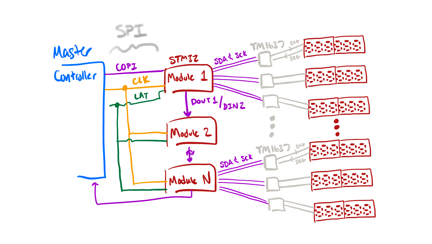
For the testing prototype I dropped the "daisy-chainable" modules idea since it seems like setting up the two DMA channels for full duplex send/receive (Shift-Register like), allowing us to "shift-through" data may be difficult with the low performance C0 series STM32 chips, see here. However, this is a key part of the "extensibility" goal of the project, so it will have to be revisited.
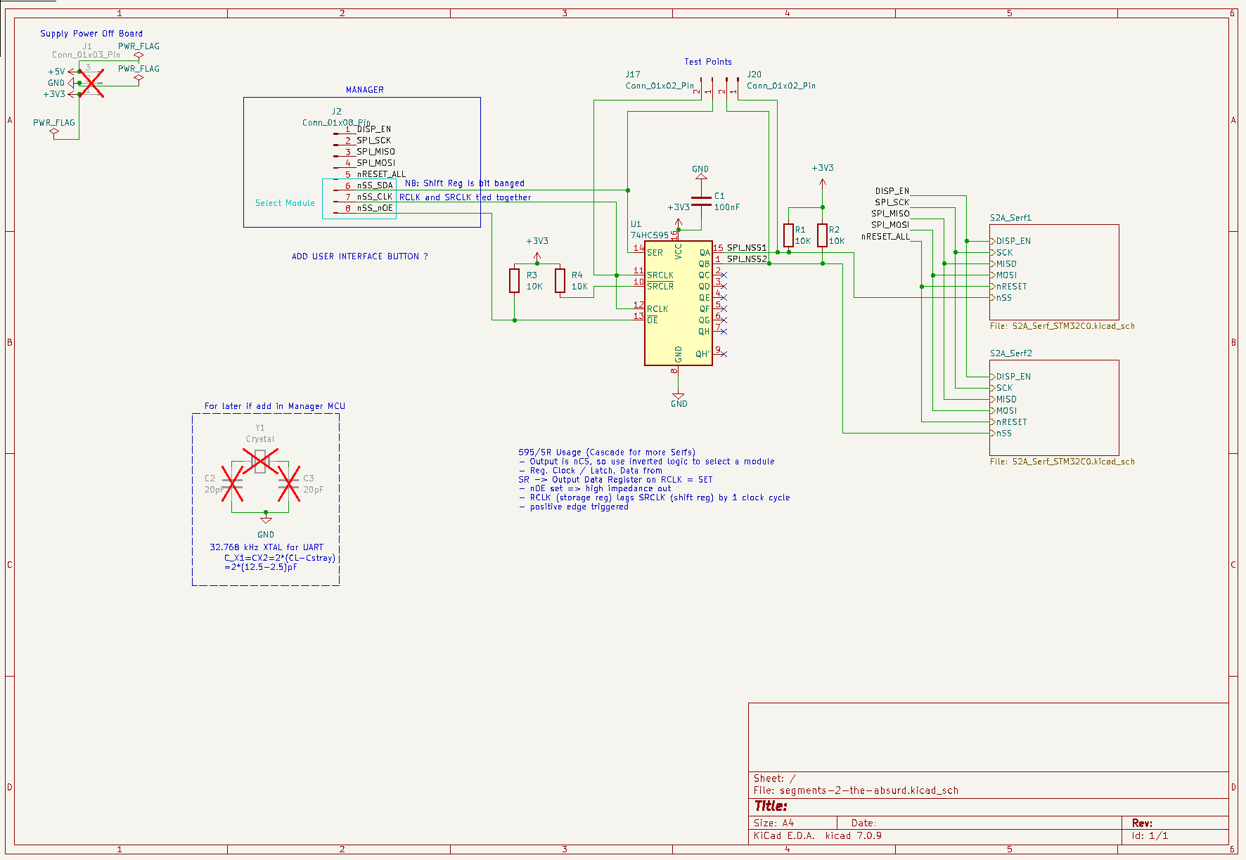
The architecture of the testing prototype is as shown:
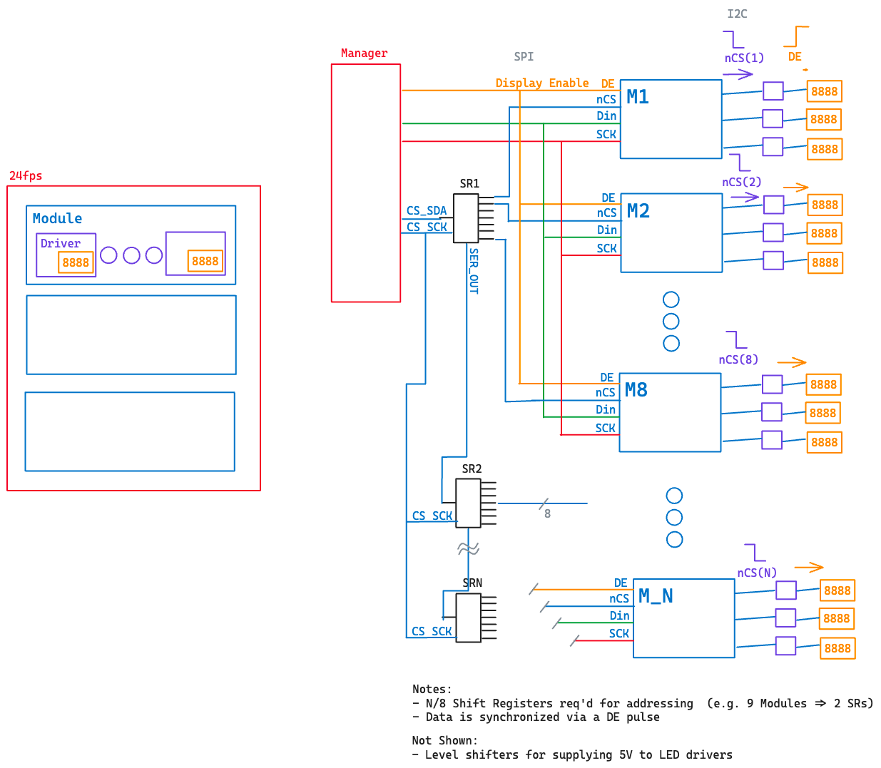
The "Manager" is just a pin header for a micro to send the LED serial data to the Modules; a shift register (SR) is added as a GPIO expander for addressing, and since the SRs can be daisy-chained without additional MCU GPIO pins it is technically extensible.
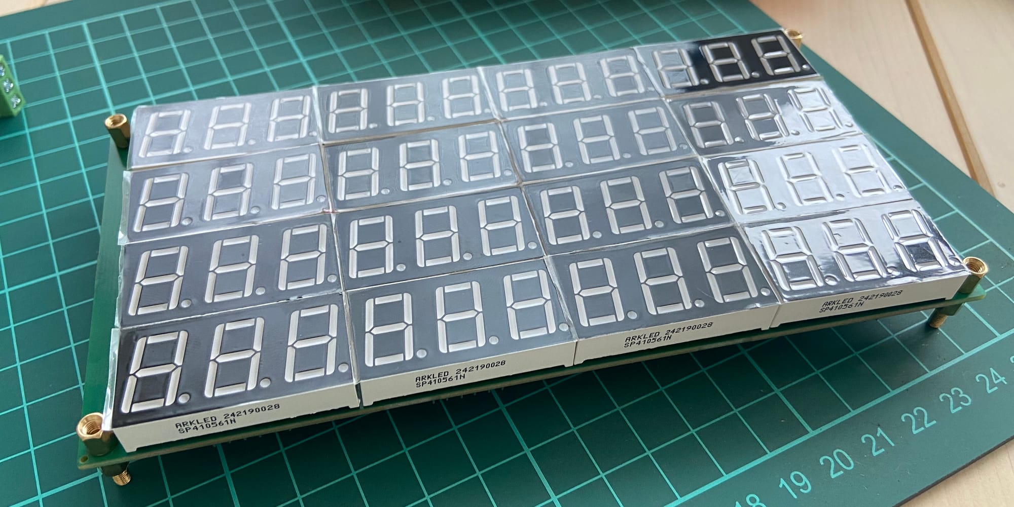
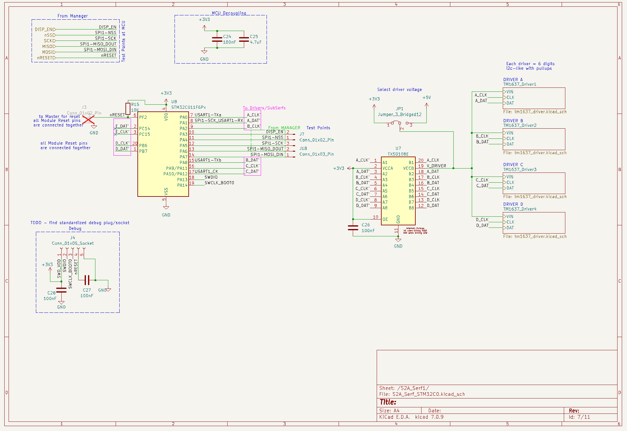
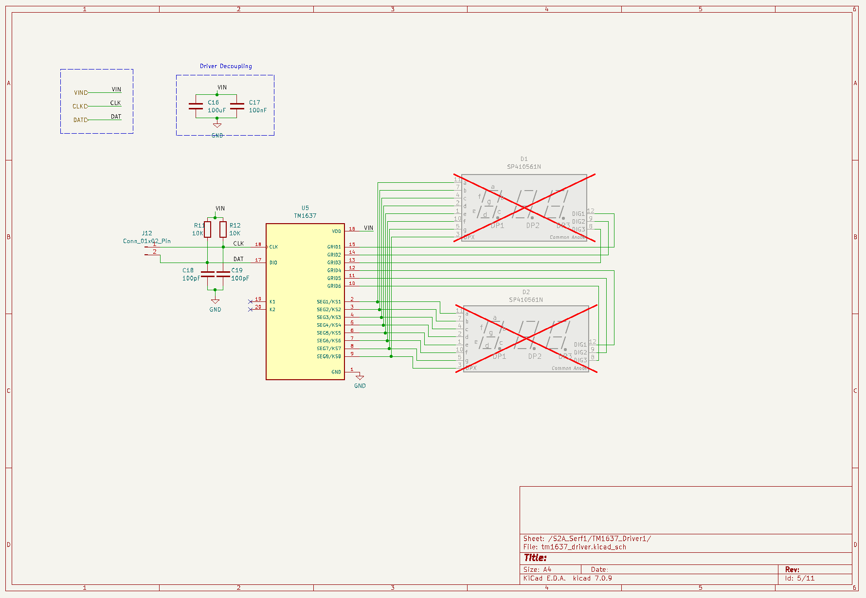
The Modules center around a single STM32 each driving (4) x TM1637 LED drivers. Each TM1637 can drive a maximum of 6 digits, which I've utilized here by using two 3-digit displays (not shown). Thus each module controls 6*4=24 digits.
Timing
Each module will receive the serial data corresponding to the LED segments it is driving and store it using DMA into memory-mapped SRAM. Once the SPI serial data transfer is complete the module will shift out the data over I2C as required by the TM1637 driver. Note that we can send the data to the driver chips without displaying the data as there is a special display command code that we will send later once the Module receives a Display Enable command from the Manager. This allows us to send the display command to the driver chips in "faux-parallel" by interleaving the slower 250kbps I2C max speed of the TM1637 driver, resulting in all the segments updating at once (one hopes).
The timing diagram for a 24fps update rate is as shown:
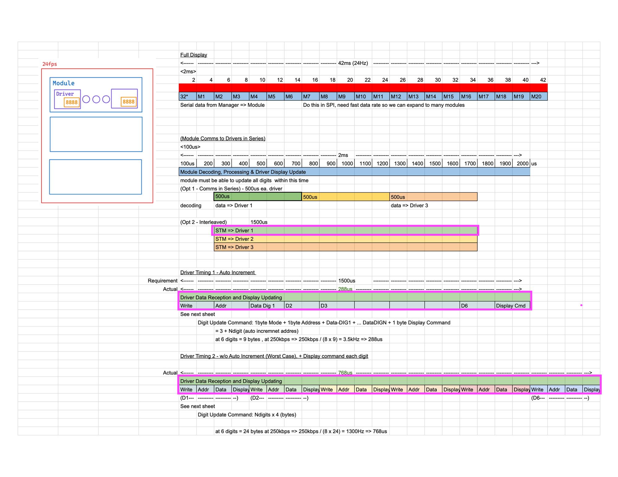
For a 24Hz display refresh rate, transmitting data to each module in series can take a maximum of 42ms/N_modules or e.g. 2ms for 21 modules. Within the 2ms we just have to send the data over SPI to the STM32 Module. Here since we are not including brightness data it is just bits = (no. segments) * (no. digits) = 8 * 6 = 48 bits or 6 bytes per module. The data is stored in memory mapped SRAM and all segment data should be shifted out to the drivers after the SPI transfer from the Manager is finished. Note that the displays will not be updated at this moment, but only after the "Display Enable" pin is set will the MCU send the proper Display Update command to the LED drivers.
Each MCU module is driving 3 of the TM1637 driver chips at a max speed of 250kbps per the datasheet so it is most efficient to interleave the serial output to all three at the same time. Continuing with the rough calculation for a 21 module example above, this means we can get about 1500us with 250us of buffer on each side to fit within the 2ms period. The auto incrementing setting of the TM1637 chip auto-increments the address for each byte, so we just have to send the address corresponding to the first digit we want to update. To update 6 digits means we would send 9 bytes. The first two bytes are the write command and address bytes, the next six are the data with auto-incrementing enabled, and the last is the display command, which will update the displays with the data [[1]].

[[1]]: The MCU/module will send this display update command when the Display Enable pin is set, and all the displays should be updated nearly simultaneously
So \( (250\text{kbps}/8)^{-1}\times 9\text{ bytes} \) gives 288us to update 6 digits. The theoretical display update at this speed is about 3.5kHz. This gives the theoretical maximum size display to be
$$N_{modules,max} = \frac{3.5\text{ kHz}}{24\text{ Hz}} \approx 145\text{ modules} \\ \Rightarrow 145\times 18 \approx 2600 \text{ digits}$$
This is approximately a 50 x 50 digit wall, although this doesn't include the internal delay of the driver chip to drive the digits. Each display is about 19mm tall gives almost a meter by meter wall. Note the TM1638, which can drive up to 10 digits, can run twice as fast. Just if you were wondering 😉.
Component Cost
Component costs are shown below for the major components sourced via LCSC since that is where I could find the TM1637 the cheapest. This doesn't include discretes like resistors and capacitors or the PCB fabrication price.
| Part | Cost | Qty per Module | Cost Per Module |
|---|---|---|---|
| 3-digit Display | $0.38 | 8 | $3.04 |
| Shift Register | $0.06 | N/8 | negligible |
| TM1637 LED Driver | $0.17 | 4 | $0.68 |
| STM32C011F6Px | $0.77 | 1 | $0.77 |
| TXS0108E Level Shifter | $0.32 | 1 | $0.32 |
| Total (per module) | $4.81 | ||
| Total (per digit) | $0.20 |
PCB Layout
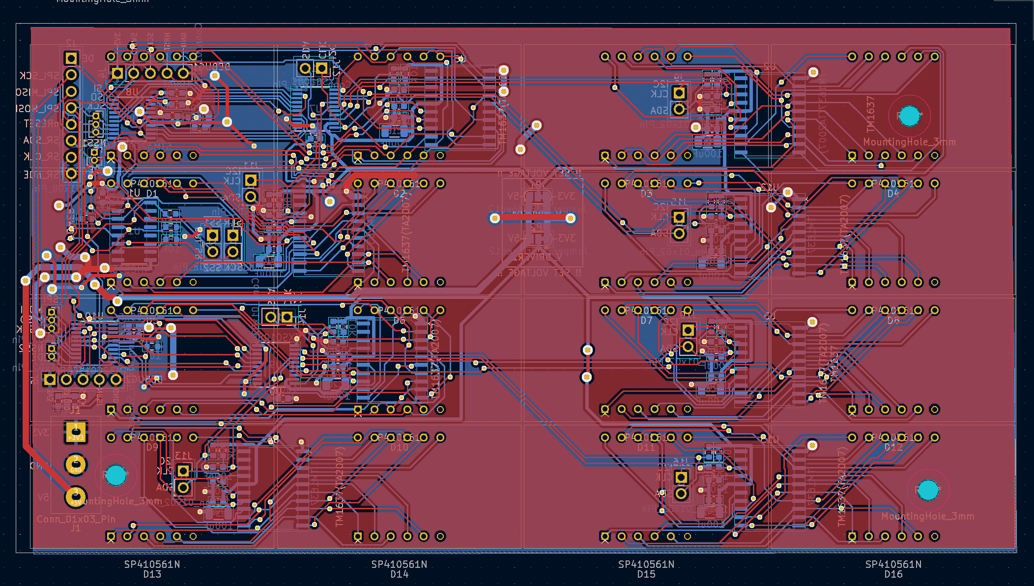
I added a bunch of 0.1"/2.54mm pitch header pins for testing purposes and for the main controller/Manager. In tight places I had to go down to 0.05"/1.27mm headers when I wanted to keep the test point close to the STM32 chip.
One layout mistake I made was to route power last. I started with the critical clock and data traces but then kept going and going until I finally got to power last... the increased track width forced me to move a lot of already-placed vias and continuously re-stitch power planes as I moved things around 🤦.
As always, footprint datasheets were scrutinized thrice over, but only custom footprints for the TM1637 and the Seven Segment Displays were needed (the other footprints were found in the KiCad default libraries).
- TXS1080E Level Shifter & STM32C0: TSSOP-20, Body=4.4x6.5mm, Pin Pitch=0.65mm
- TM1637: Custom, SOC-20, Body=12.6x7.5mm, Pin Width = 1.27mm; Pin Width =0.44mm
- Seven Segment Displays: Custom, pin pitch is 2.54mm apart (3 digit footprint is same as 4 digit with one pin unconnected)
Power Supply Voltage Levels
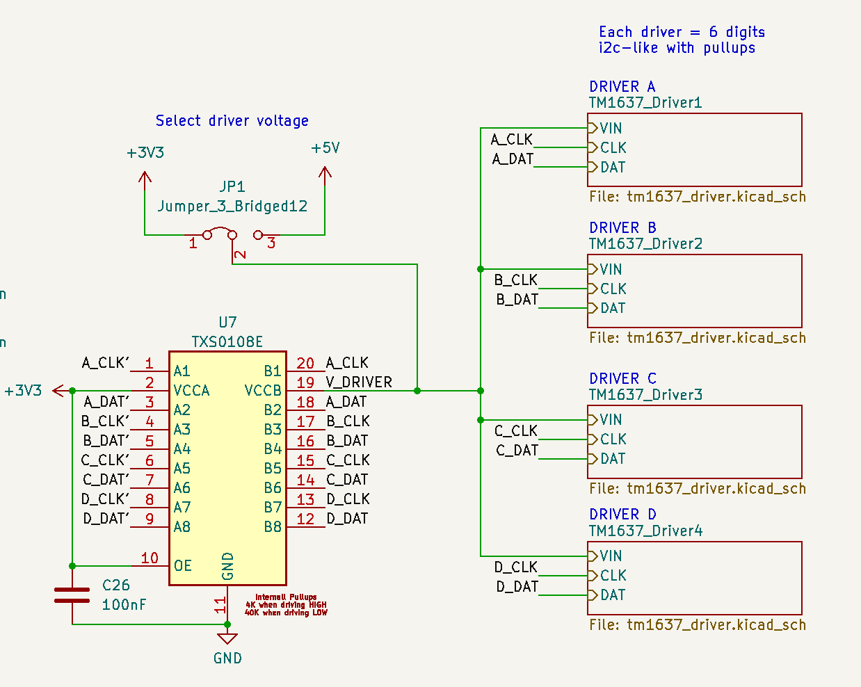
Although the red-LEDs with their ~2V voltage drop should be able to be driven by the TM1637 at a 3V3 supply, for testing purposes I added in a 5V rail via a solderable jumper. The driver voltage is set by soldering either the 5V side or the 3V3 side. Both 5V and 3V need to be provided separately via screw terminals (no converter included).

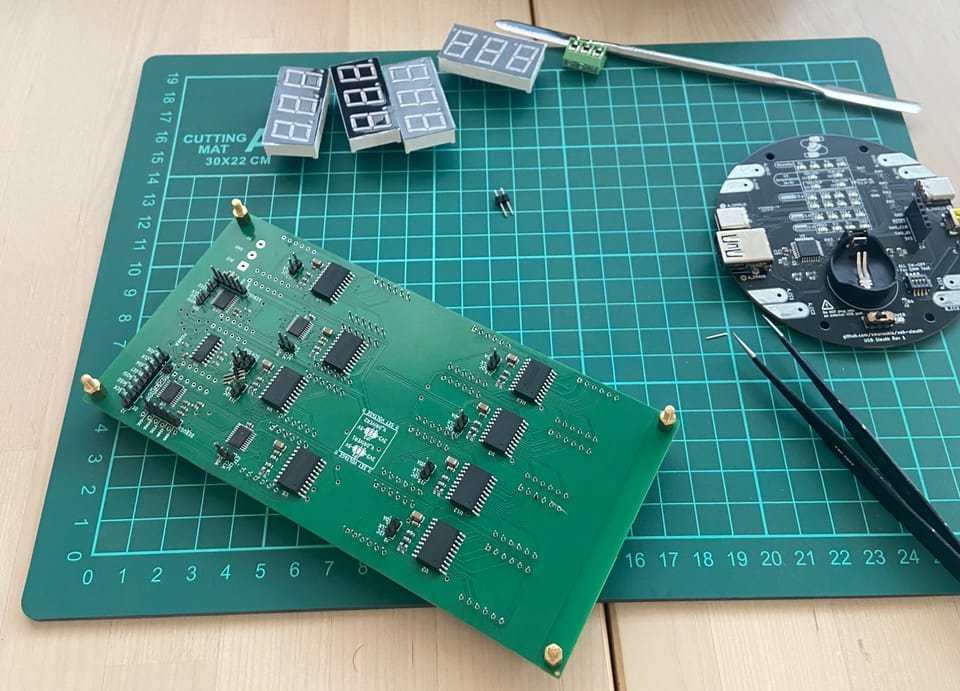
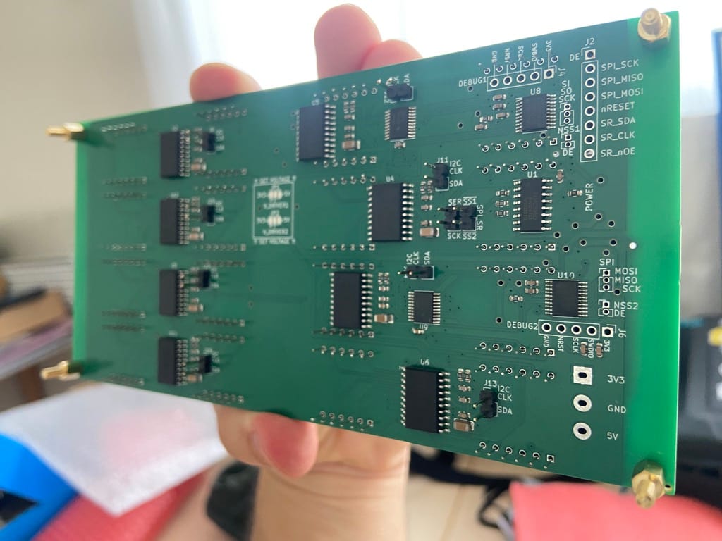
Here is the finished board without the headers soldered:
With the displays:
Prototype Schematics
Here are some schematics:
Next Up
Next up will be testing the hardware and writing the firmware for the Modules as well as looking into the Manager controller firmware (decoding GIF images/etc. and converting to the serial bit stream).
The final hardware will change depending on the timing and voltage requirements, as well as being made more modular.
A stretch goal would be to test firmware that allows for daisy-chaining the STM32 modules instead of using a SS chip select pin with the Shift Register. This would allow the system to work more like the daisy-chainable WS2811 or APA102 RGB LED driver chips.
