USB Sleuth Cable Tester
Overview
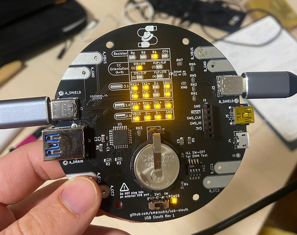
After being inspired by various USB cable testers, I decided to build my own to get familiar with STM32, KiCad and the USB-C standard. Mostly it was a hardware fork of this hackaday project that had a schematic but no firmware.
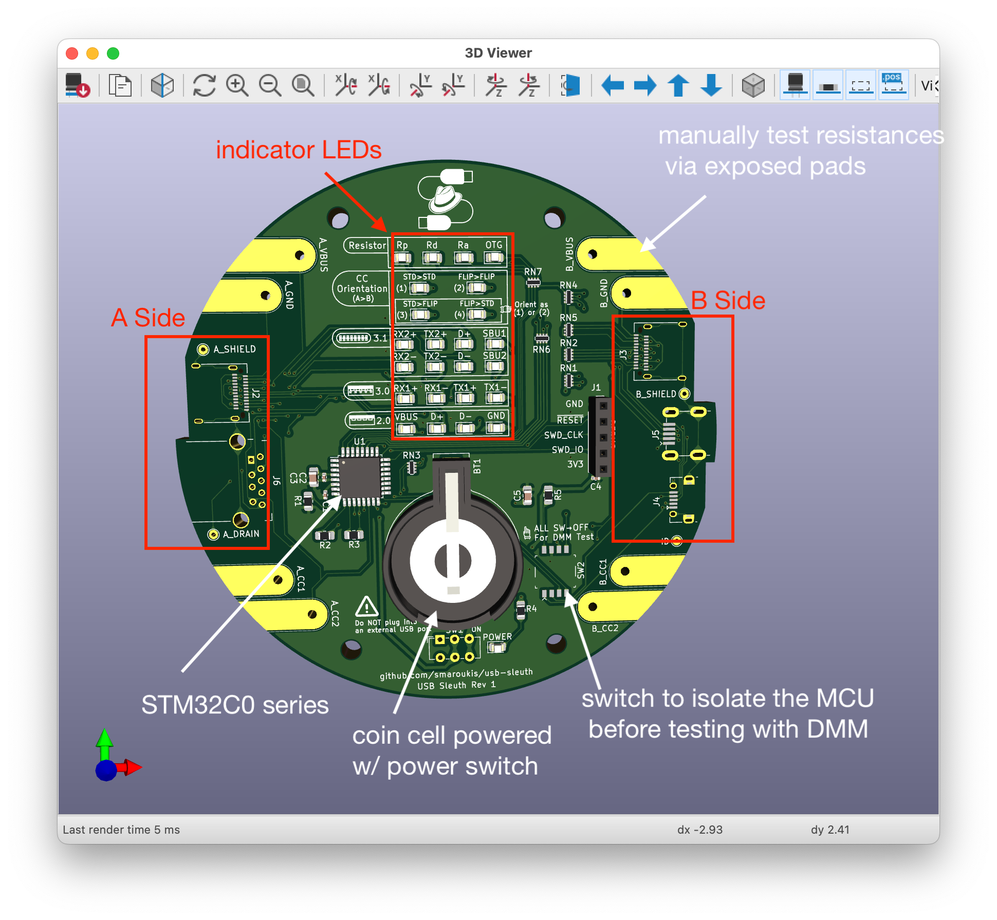
The device has some benefits over a simple continuity tester:
- displays the as-plugged orientation of the 4 different possibilities of the USB-C to C cable
- detects pullup and pulldown resistors on the CC lines as required by the USB standard for legacy cables
- identifies active cable with E marker (via the pulldown resistor present on VCONN)
- doesn't apply a +V to the Ground line/pin, instead it uses a MCU to test the presence of a connected ground wire
- exposes various pins to test cable and internal resistors manually with a DMM
I went through JLCPCB to manufacture the boards, choosing parts from their library coming from LCSC. The C code uses the STM32 HAL libraries, a further improvement would be to port this to lower level and publish a CMake file so that it is less reliant on the STM32CubeIDE.
Detailed documentation, firmware, and KiCad files are in the README on github. This blog post will describe more of my learnings and gotchas than the technical details of the project.
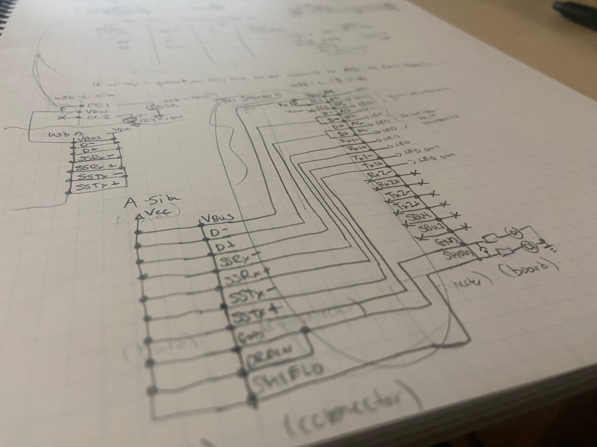
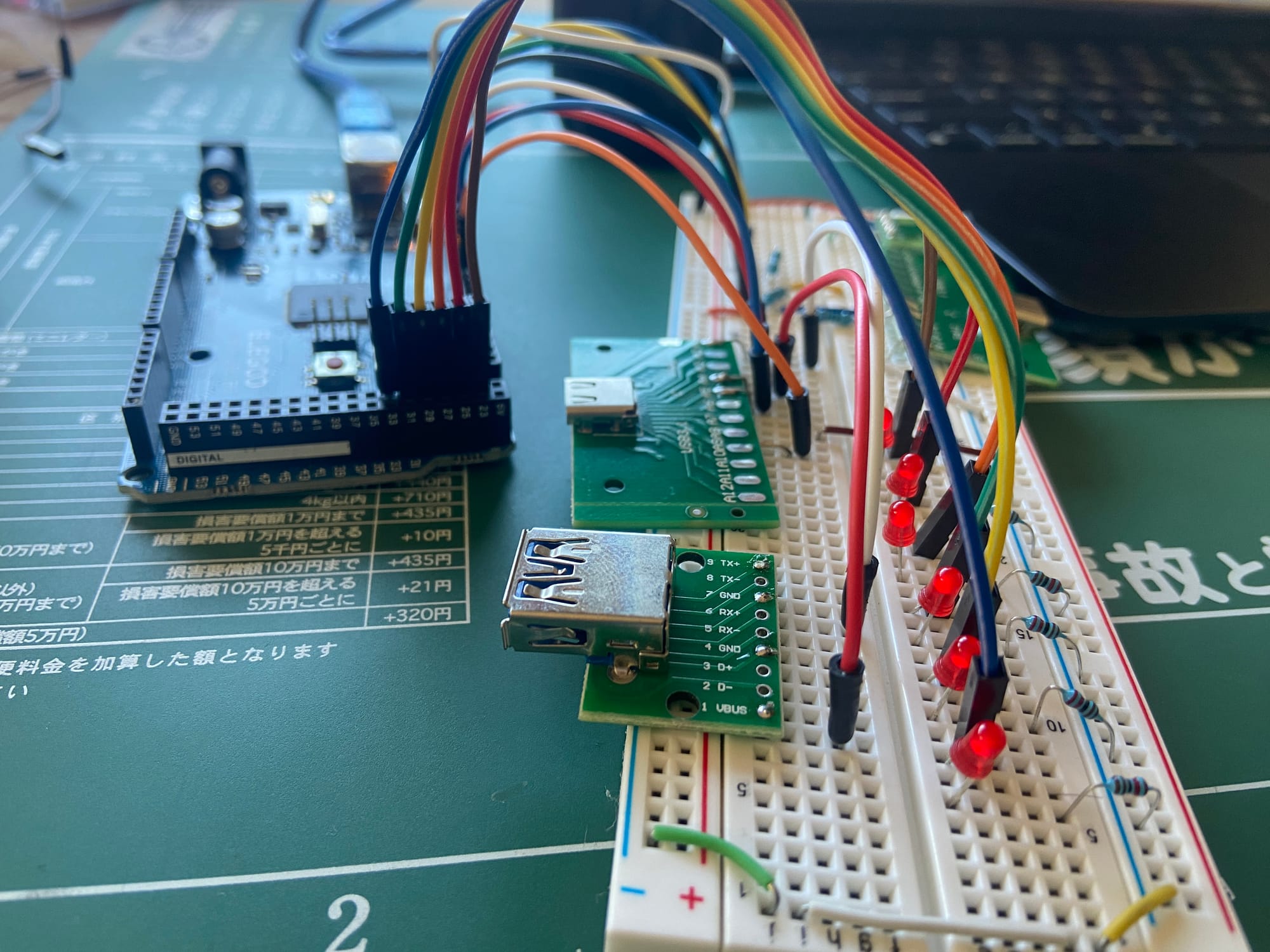
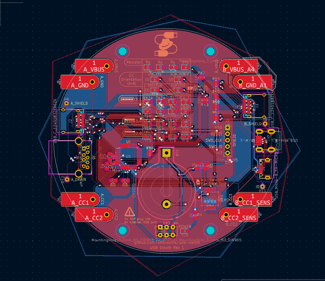
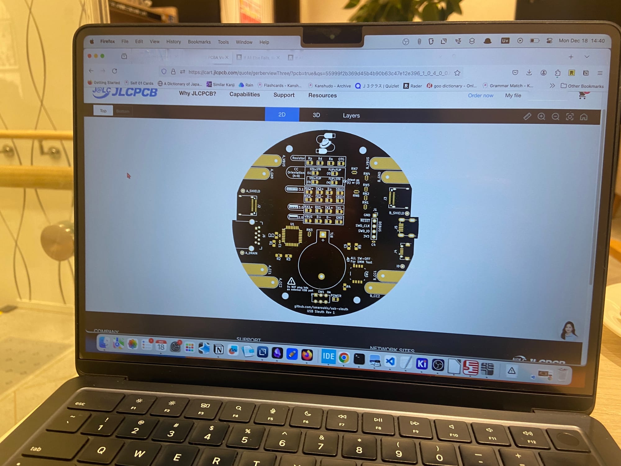
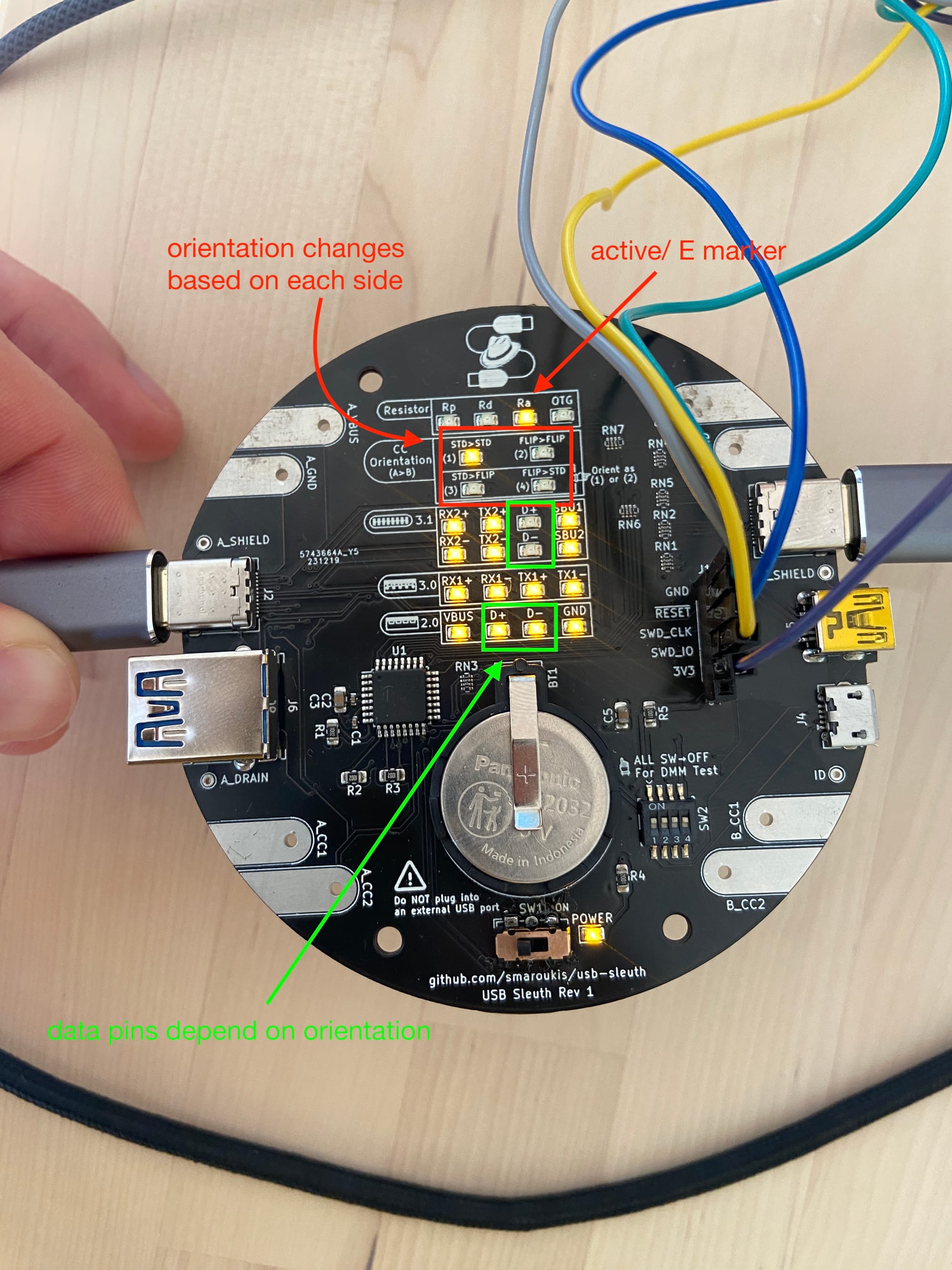
Design, prototyping, pcb layout, and doing the final hand placements.
Interesting Tidbits
Analog vs digital read on cable internal resistors: A USB A to C cable will have a 56K internal pullup from the CC pin to VBUS (since in the USB-C standard the CC pin on the host side should be pulled up to identify as a host, but of course the USB-A side doesn't have the CC pin, so it must be pulled up in the cable itself).
We test this as in the following schematic by pulling the B-side CC control pin, BCC1_CTRL , to 0V through a 1oK resistor and measuring the voltage at the divider point, BCC1_Sense. Note here we can't use a digital read.

BCC1_CTRL→0V. If an analog read of BCC1_Sens is greater than 0.15*VBUS, then the pull up is present. In the USB B-to-C case, the B side is pulled down to GND pin with a 5.1K resistor. To test, instead of pulling BCC1_CTRL to 0V, we pull ACC1 high through an internal pullup. Since the internal pullup is ~50K, about 10 times weaker than the 5.1K pulldown, we can use a digital read (==LOW) to check if the pulldown is present.

This is also documented in the README.
Key Learnings:
- Custom footprints and multi-unit symbols: Custom footprints are a pain at first, but better to pull that tooth out sooner than later (or end up with a misaligned part); multi unit symbols are a cool feature to make it easy to draw a 4 pole DIP switch as separate switches in the schematic but link to a single component.
- Double check minimum clearances before routing traces: I had my minimum via size wrong from the start, which required a rework of all the traces off of the USB-C ports.
- USB cable standards and pullup/pulldown resistor configurations: A-to-C will have a 56K pullup, B-to-C will have a 5K1 pulldown, and an active C-to-C cable will have a ~1K pulldown.
- Existence of ESD diodes on MCU GPIO pins: I added an isolation switch to use during DMM testing of the resistor values, to avoid a path through ESD diodes on the GPIO pins causing bad readings. Once receiving the boards, the switch positions didn't have an impact on the measurements, so they could be removed in future hardware versions.
- Generating correct BOM and gerber files: In KiCad for JLCPCB, I used the Fabrication Toolkit plugin, edited a bit of the python file, and used the DNP field of the KiCad schematic viewer to mark hand placed components which would be excluded from the auto generated BOM.
- Using commodity parts with JLCPCB/fab houses: Once I found out how to search for them using JLCPCB/LCSC's abysmal parameter search, I tried to use commodity ("basic") parts since reels of these are already loaded on the pick 'n place machine; for each "extended" part number you pay a loading fee of $3 → this fee can be avoided for things like resistors, capacitors and LEDs but not for parts like USB receptacles or resistor arrays.
More Specific Learnings
- JLCPCB viewer doesn't have the correct orientation of the components - they will rotate them correctly on their side (but I paid an extra dollar or two for the final production file to be sent for my approval)
- I had a lot of back and forth between JLCPCB engineers about my pads sticking outside of the board edge layer – which I designed that way just to be clipped by the board edge layer.
- Renaming files and folders in the KiCad project is a bit of a workaround – for example when I wanted to rename the directory with the custom footprints, the easiest way is to rename the file itself and then use e.g. VSCode to "find/replace" all occurrences of the footprint path.
Scope Creep
- differential pairs and the drain wire in USB 3.0 (the drain wire is a return signal for any unbalance in the differential signal, and as a heavier conductor to ground the thin shield to divert large EMI spikes to ground)
- taller SMD capacitors (vs resistors) requires a wider pad in order to get a solder fillet all the way to the top of component (and avoid tombstoning)
- multi unit symbols in KiCad - useful for the creating 4 individual schematic switches for the 4 pole DIP switch.
Project Timeline Highlights:
- Feb 3: Published Hackaday.io project and was featured on Hackaday.com
- Jan 27: STM32 HAL code finished and all tests working. Rev 1 complete 🥳
- Jan 17: Testing and porting Arduino code to STM32 HAL C.
- Jan 3: Boards delivered.
- December 21: Back and forth with JLCPCB about pads extending beyond the board edge resolved.
- December 18: Sent the project for production.
- December 15: BOM generation using Fabrication Outputs plugin.
- December 13: USB port custom footprint edits, footprint calculator, and final edits.
- December 11: Second day of routing, with challenges in USB-C routing.
- December 8: PCB layout updates and considerations for taller SMD capacitors.
- December 5: Investigation of ESD diodes and DMM current injection paths for Ra/Rd/Rp.
- November 27: Hardware test for CC orientation, pull-down/up.
- November 17: Continued layout with logic for testing, wired up to Arduino.
- November 10: Bought USB-C and USB-A breakout board for testing.
- November 9: Research on USB pinouts, grounding, and differential signals.